1. Material Basics and Structural Attributes of Alumina Ceramics
1.1 Crystallographic and Compositional Basis of α-Alumina
(Alumina Ceramic Substrates)
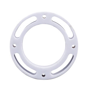
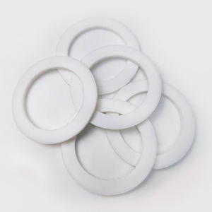
Alumina ceramic substrates, mostly made up of light weight aluminum oxide (Al ₂ O TWO), work as the foundation of modern electronic product packaging as a result of their extraordinary equilibrium of electric insulation, thermal stability, mechanical strength, and manufacturability.
One of the most thermodynamically secure stage of alumina at heats is corundum, or α-Al ₂ O THREE, which takes shape in a hexagonal close-packed oxygen latticework with aluminum ions inhabiting two-thirds of the octahedral interstitial websites.
This thick atomic plan conveys high hardness (Mohs 9), exceptional wear resistance, and solid chemical inertness, making α-alumina ideal for severe operating environments.
Industrial substrates usually have 90– 99.8% Al Two O SIX, with small enhancements of silica (SiO TWO), magnesia (MgO), or unusual planet oxides made use of as sintering aids to promote densification and control grain development during high-temperature handling.
Greater purity qualities (e.g., 99.5% and above) exhibit superior electric resistivity and thermal conductivity, while reduced pureness variations (90– 96%) use affordable remedies for much less requiring applications.
1.2 Microstructure and Problem Engineering for Electronic Dependability
The efficiency of alumina substratums in digital systems is seriously based on microstructural harmony and flaw reduction.
A fine, equiaxed grain framework– typically varying from 1 to 10 micrometers– ensures mechanical honesty and minimizes the probability of crack propagation under thermal or mechanical stress and anxiety.
Porosity, particularly interconnected or surface-connected pores, need to be reduced as it weakens both mechanical stamina and dielectric performance.
Advanced processing techniques such as tape casting, isostatic pushing, and regulated sintering in air or controlled atmospheres enable the production of substratums with near-theoretical density (> 99.5%) and surface roughness listed below 0.5 µm, vital for thin-film metallization and cable bonding.
Furthermore, impurity partition at grain limits can lead to leakage currents or electrochemical migration under prejudice, necessitating strict control over basic material pureness and sintering conditions to make sure lasting integrity in damp or high-voltage atmospheres.
2. Production Processes and Substratum Construction Technologies
( Alumina Ceramic Substrates)
2.1 Tape Spreading and Eco-friendly Body Processing
The manufacturing of alumina ceramic substrates starts with the preparation of an extremely distributed slurry containing submicron Al two O ₃ powder, natural binders, plasticizers, dispersants, and solvents.
This slurry is processed by means of tape spreading– a continual technique where the suspension is topped a relocating carrier film utilizing an accuracy doctor blade to accomplish consistent density, normally in between 0.1 mm and 1.0 mm.
After solvent dissipation, the resulting “eco-friendly tape” is versatile and can be punched, drilled, or laser-cut to develop through holes for upright interconnections.
Multiple layers may be laminated to produce multilayer substrates for complex circuit integration, although the majority of commercial applications utilize single-layer setups due to set you back and thermal development factors to consider.
The green tapes are then thoroughly debound to remove natural additives through managed thermal decomposition prior to final sintering.
2.2 Sintering and Metallization for Circuit Assimilation
Sintering is conducted in air at temperature levels between 1550 ° C and 1650 ° C, where solid-state diffusion drives pore elimination and grain coarsening to accomplish complete densification.
The linear shrinkage throughout sintering– usually 15– 20%– need to be precisely forecasted and compensated for in the design of green tapes to ensure dimensional precision of the last substratum.
Following sintering, metallization is applied to form conductive traces, pads, and vias.
Two main approaches control: thick-film printing and thin-film deposition.
In thick-film technology, pastes including metal powders (e.g., tungsten, molybdenum, or silver-palladium alloys) are screen-printed onto the substrate and co-fired in a lowering atmosphere to create robust, high-adhesion conductors.
For high-density or high-frequency applications, thin-film processes such as sputtering or dissipation are used to deposit bond layers (e.g., titanium or chromium) adhered to by copper or gold, allowing sub-micron pattern by means of photolithography.
Vias are filled with conductive pastes and fired to develop electrical affiliations in between layers in multilayer styles.
3. Practical Residences and Performance Metrics in Electronic Systems
3.1 Thermal and Electrical Behavior Under Operational Tension
Alumina substrates are treasured for their beneficial mix of moderate thermal conductivity (20– 35 W/m · K for 96– 99.8% Al ₂ O FIVE), which enables effective warmth dissipation from power devices, and high quantity resistivity (> 10 ¹⁴ Ω · cm), making certain very little leak current.
Their dielectric consistent (εᵣ ≈ 9– 10 at 1 MHz) is stable over a broad temperature and regularity range, making them ideal for high-frequency circuits approximately numerous ghzs, although lower-κ materials like light weight aluminum nitride are favored for mm-wave applications.
The coefficient of thermal development (CTE) of alumina (~ 6.8– 7.2 ppm/K) is fairly well-matched to that of silicon (~ 3 ppm/K) and particular packaging alloys, minimizing thermo-mechanical stress throughout device procedure and thermal biking.
Nonetheless, the CTE inequality with silicon remains a problem in flip-chip and direct die-attach arrangements, commonly requiring certified interposers or underfill materials to minimize exhaustion failing.
3.2 Mechanical Effectiveness and Environmental Longevity
Mechanically, alumina substratums exhibit high flexural toughness (300– 400 MPa) and superb dimensional stability under lots, allowing their use in ruggedized electronics for aerospace, automotive, and industrial control systems.
They are resistant to vibration, shock, and creep at raised temperature levels, maintaining architectural stability as much as 1500 ° C in inert environments.
In moist atmospheres, high-purity alumina reveals marginal wetness absorption and outstanding resistance to ion movement, ensuring lasting reliability in outdoor and high-humidity applications.
Surface area firmness additionally safeguards versus mechanical damages throughout handling and assembly, although care needs to be taken to prevent edge cracking as a result of fundamental brittleness.
4. Industrial Applications and Technological Influence Throughout Sectors
4.1 Power Electronics, RF Modules, and Automotive Solutions
Alumina ceramic substratums are ubiquitous in power digital components, consisting of protected gate bipolar transistors (IGBTs), MOSFETs, and rectifiers, where they offer electrical seclusion while assisting in warm transfer to heat sinks.
In superhigh frequency (RF) and microwave circuits, they function as provider systems for hybrid incorporated circuits (HICs), surface area acoustic wave (SAW) filters, and antenna feed networks because of their secure dielectric buildings and low loss tangent.
In the automobile industry, alumina substrates are utilized in engine control devices (ECUs), sensing unit bundles, and electric automobile (EV) power converters, where they endure heats, thermal cycling, and exposure to destructive fluids.
Their dependability under extreme conditions makes them indispensable for safety-critical systems such as anti-lock stopping (ABDOMINAL) and progressed motorist support systems (ADAS).
4.2 Clinical Devices, Aerospace, and Emerging Micro-Electro-Mechanical Equipments
Beyond consumer and commercial electronic devices, alumina substratums are employed in implantable clinical gadgets such as pacemakers and neurostimulators, where hermetic sealing and biocompatibility are extremely important.
In aerospace and defense, they are used in avionics, radar systems, and satellite interaction modules as a result of their radiation resistance and security in vacuum settings.
Moreover, alumina is increasingly made use of as a structural and shielding platform in micro-electro-mechanical systems (MEMS), including stress sensors, accelerometers, and microfluidic tools, where its chemical inertness and compatibility with thin-film handling are beneficial.
As electronic systems continue to require greater power thickness, miniaturization, and dependability under extreme problems, alumina ceramic substrates continue to be a keystone product, connecting the void between efficiency, expense, and manufacturability in advanced electronic product packaging.
5. Vendor
Alumina Technology Co., Ltd focus on the research and development, production and sales of aluminum oxide powder, aluminum oxide products, aluminum oxide crucible, etc., serving the electronics, ceramics, chemical and other industries. Since its establishment in 2005, the company has been committed to providing customers with the best products and services. If you are looking for high quality alumina silica, please feel free to contact us. (nanotrun@yahoo.com)
Tags: Alumina Ceramic Substrates, Alumina Ceramics, alumina
All articles and pictures are from the Internet. If there are any copyright issues, please contact us in time to delete.
Inquiry us